Hello, fellow students! I’m Son, a beginner in KiCad and SolidWorks. The steps below will help you get familiar with KiCad or SolidWorks quickly. I hope that after following these basic steps, you’ll be able to start building simple prototypes.
Date: 3/11/2025
Revision: 12/23/2025
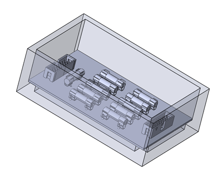
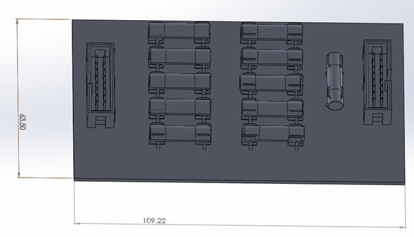
Final Product
Kicad
Requirement
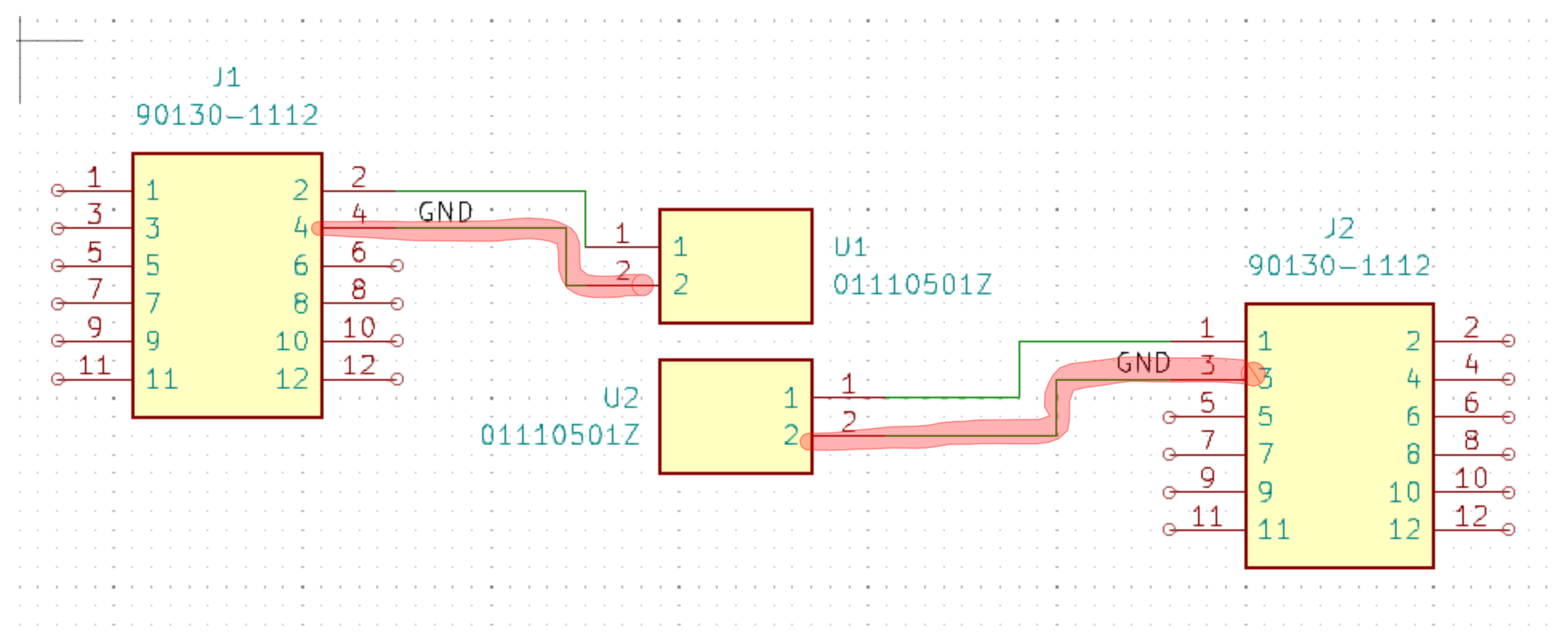
First, we need to define what we’re designing. Our goal is to create a fuse box for voltage sense lines.
We have a total of 11 sense lines, and each one must have a fuse to protect the end device or downstream device. Our device can handle up to 300mA at peak, so choosing a 500mA fuse seems like a good option.
Next, we’ll select a connector and choose the appropriate fuse size along with a suitable fuse holder. Now, let’s go shopping!
Shopping
Here are four websites that I often use:
- Digikey: Electronic component, sometimes it is cheaper than Amazon
- Octopart: to get 3D model and Kicad symbol, footprint
- Ultralibrarian: Similar to octopart that provide both 3D model and Kicad symbol
- Amazon: get other part that cheaper than digikey
- McMasterCarr: great website for mechanical parts. It also has good technical information
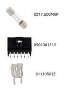
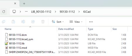
These are three components that I pick. Also, please check the pitch size to avoid ordering parts that are not compatible on our perfboard.
By standard the pitch size of perfboard is 0.1 in or 2.54mm.

Get the CAD, Symbols and Footprint files
Next, I will go to octopart to download the necessary files Octopart
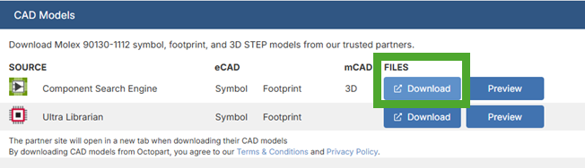
This is the files that I received
They also include 3D model file here

Importing Symbol and Footprint to Kicad
Let put everything in one folder so we can manage it easier Now open Kicad and create new project. Open Kicad Schematic Editor

On Preference select Manage Symbol Libraries,
Choose Project Specific Libraries

and add ______.kicad_sym

Now go back to Preference and select Manage Foot Print Library, add folder

Start Building
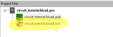
Select kicad_sch file to start editing
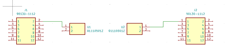
Press A to add symbol
Then we go to Tool > Annotate Schematic
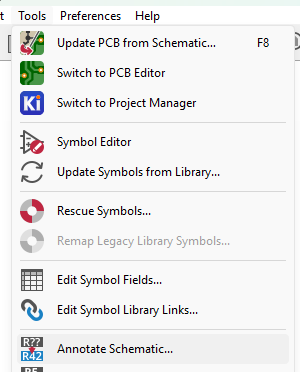
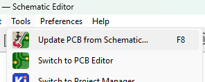
Next, we will select Update PCB from Schematic
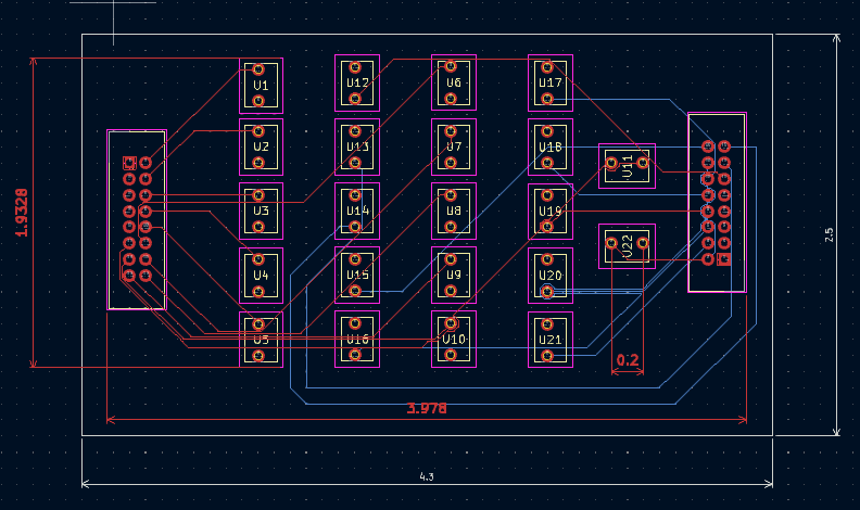
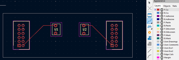
Now you can arrange components on your board, make sure fuse will fit in between two holder (0.6 in)
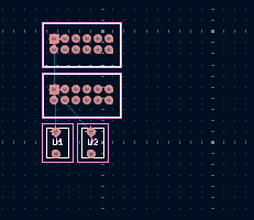
We also need to create a main board. So click on Edge.Cuts

use rectangular symbol to draw the shape of your pcb board
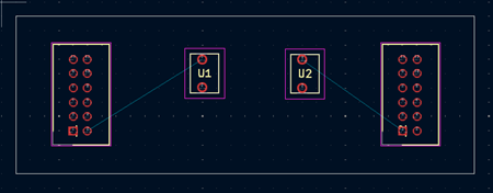
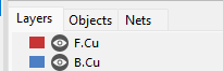
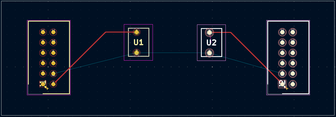
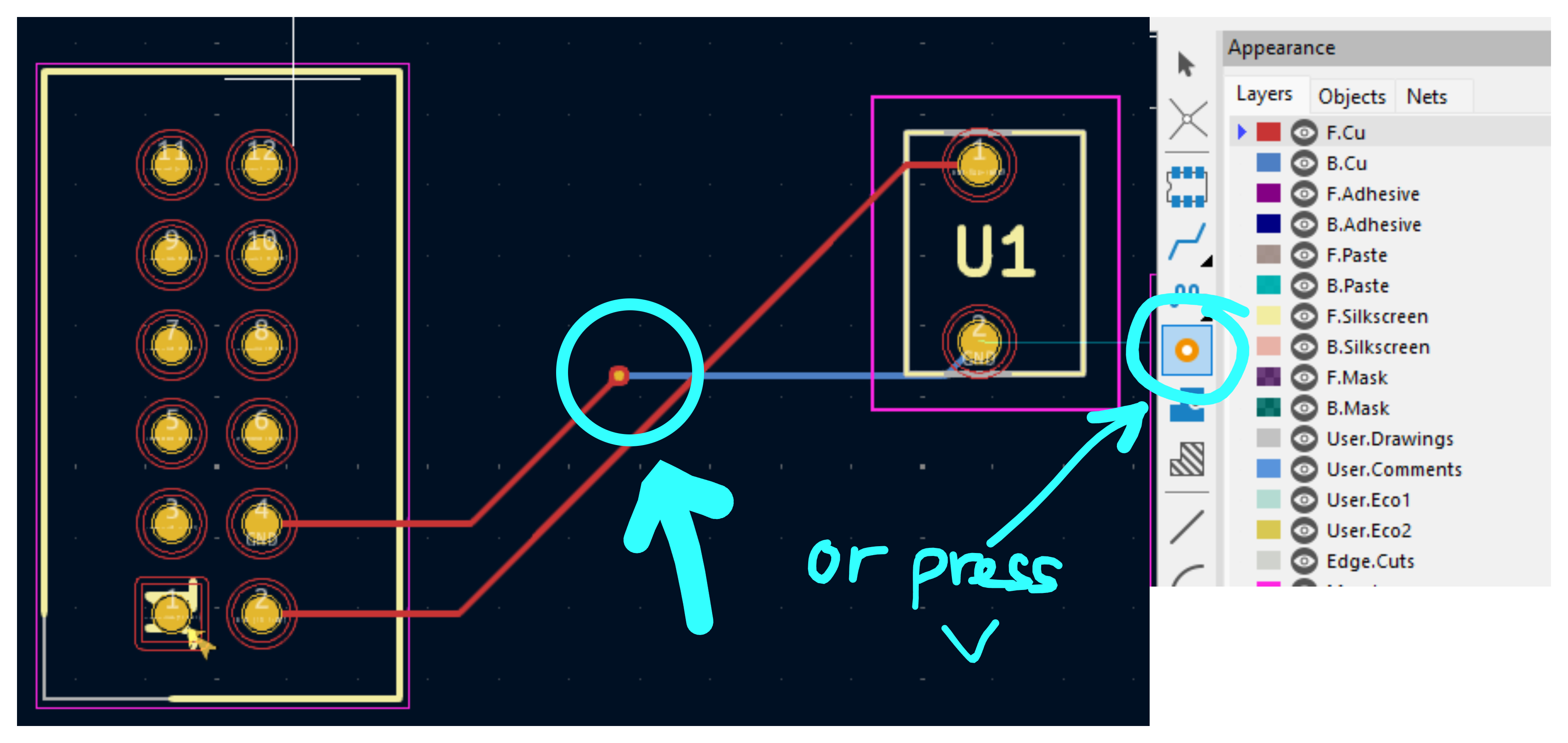
Now, we need to route copper trace. There are two layers, front and back.
I select front and start Wiring (or press X)
Now you can check your product by click on View > 3D Viewer
CONGRATULATION!!! you can design a PCB on your own
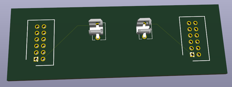
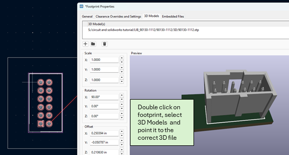
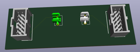
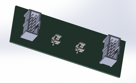
Notice that we don’t see the 3D connector here, let add it
And this is the final result after we add 3D models.
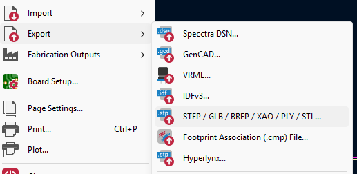
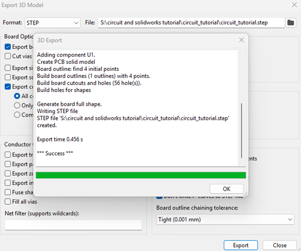
Export to Step file
Adding Copper pour (Optional)
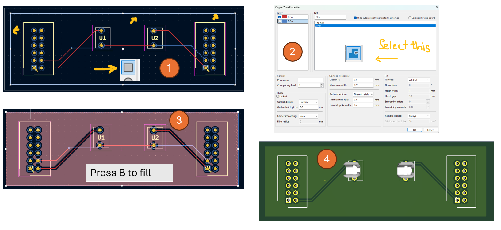
We can also add copper pour which is a copper layer on top of the FR4 to improve signal and dissipate heat. We may don’t need it in this simple circuit.
To draw a rectangular that fills the entire board, I will create a rectangular shape first (1). Then, I will select GND in (2) and then using the rectangular as a guide to draw the boundary. Next, I press B to fill the copper. The final version is shown in (4).
Adding vias to the second layer
When I add two traces (red highlighted)
The ratsnet now changes
To route the track, we can either route it on B.Cu by clicking on the B.Cu layer and route normally as in F.Cu.

Or we can use vias
SolidWorks
Navigate SolidWorks (5 mins)
Rotate: using middle button on the mouse Pan: or moving the design by pressing control button and middle button of the mouse Spacebar: fit an object into windows
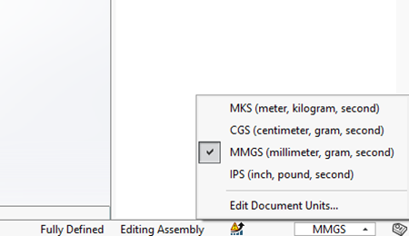
Unit in SolidWorks (1 min)
On your right-hand side, select mm as unit
Measuring
Using Smart Dimension to measure the size of an object
Let’s Start
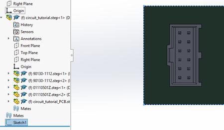
Import STEP file
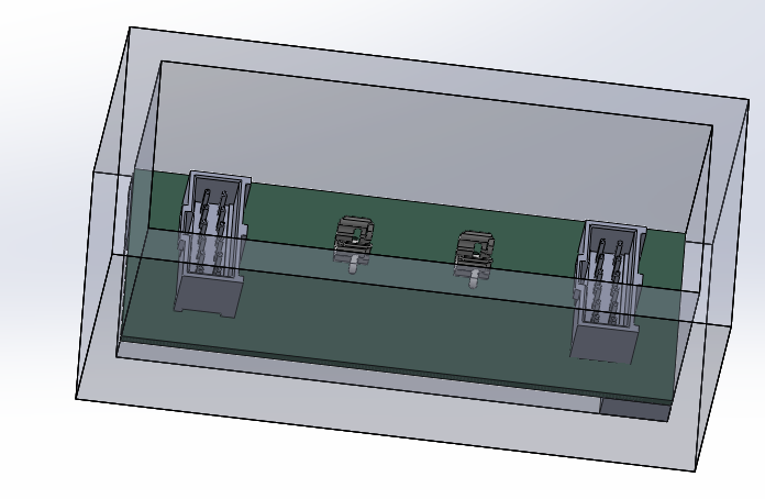
This is the circuit we design earlier
Let build a box for it; I usually search online to get an idea.
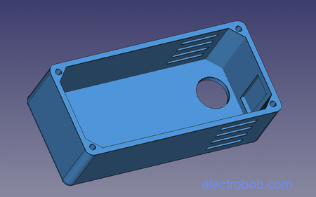
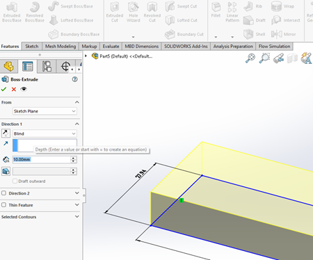
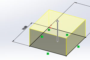
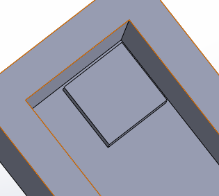
The box above looks nice but let make something simple. I want to create a box with 5mm thick and cover the pcb board. The box should have 4 leg with the height of 5mm to raise the board up. The box will be 40mm height.
Create a box
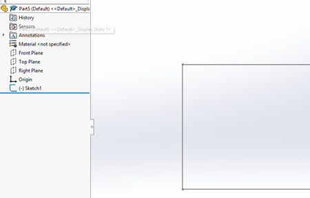
Draw a sketch around the circuit board
File > New part > Paste that sketch to top plane
Extrude that box for 40mm
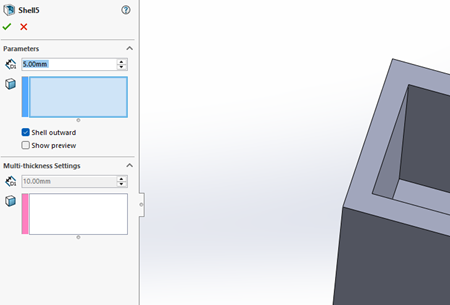
Select top surface of the box and create 5mm shell outward
Save this as box
Create a leg
File > New Part
save as leg
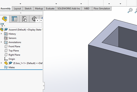
Assembly
File > new Assembly
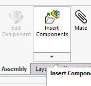
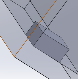
add the box
add the leg
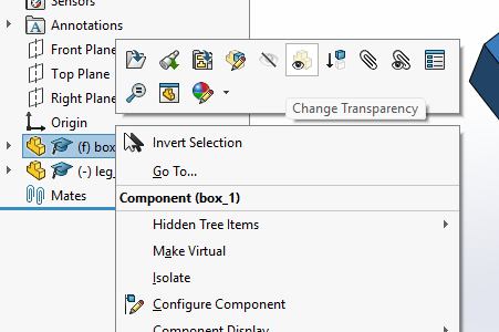
Change transparency of the box
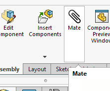
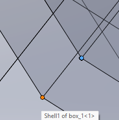
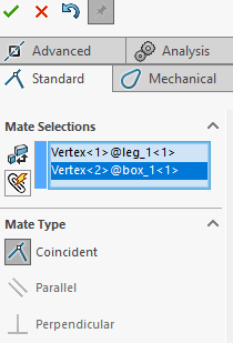
Using Mate function
CONGRATULATION!!! you have designed a simple container for your pcb
Review
We have worked through a simple example of how to design a PCB and casing using Kicad and Solidworks.
In this Example, we learned:
- Find components files including 3D, symbols and footprints.
- Kicad:
- Create a New Project
- Solidworks:
- Create a container or box
Change log
| Date | Note |
|---|---|
| 3/11 | Init doc |
| 12/23 | Add vias, copper pour |